Contact Us
Contact our corporate or local offices directly.
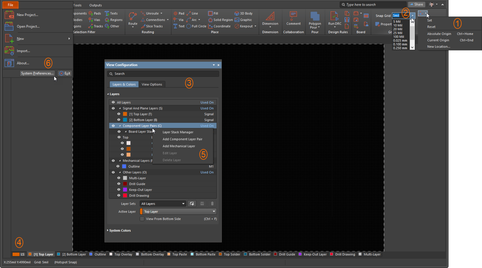
A logical continuation after creating and checking the schematic document is creating and designing the PCB. Use the File » New » PCB command to create a new PCB document. It is a good idea to configure the PCB by defining the origin (1), units, grid size (2), as well as the color display and visibility of the required layers in the View Configuration panel (3).
The Inspector panel displays information about the entire structure of the PCB for the selected layer.
To define the origin, use the following options in the Origin drop-down menu:
The active layer is specified at the bottom of the design space where all created layers are displayed according to the visibility settings determined (4). You can switch between layers sequentially using Ctrl+Shift+Mouse Wheel.
Use the Add Components Layer Pair and Add Mechanical Layer commands (5) in the View Configuration panel to add new layers. The creation of new signal layers is possible only in the Layer Stack Manager, which is described later on this page.
System settings are accessed using the File » System Preferences command (6); the PCB Editor Preferences are used for PCB system settings.
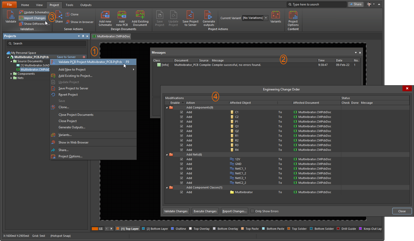
For successful synchronization of schematic and PCB, the project must be checked for errors and warnings. Use the Validate PCB Project (1) command available in the Project | Validation region or by right-clicking on the project name in the Projects panel to validate the project and access a list of violations or receive a notification regarding successful compilation/validation in the Messages panel (2) if no errors or warnings were found.
You can import changes from the schematic using the Project | Validation | Import Changes button (3). The Engineering Change Order dialog (4) opens in which you can validate the changes using the Validate Changes command. The Execute Changes command is used to apply the changes that are made.
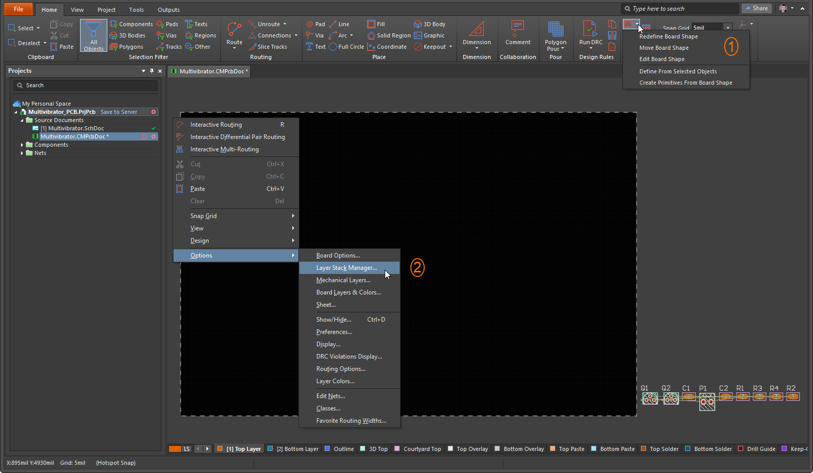
As a rule, PCB design begins with specifying the overall dimensions. You can change the PCB dimensions and geometry using the Home | Board | Board Shape drop-down commands (1).
To determine the internal structure of the board, open the Layer Stack Manager by choosing Home | Board | Layer Stack Manager or select Options » Layer Stack Manager from the right-click menu (2).
In the Layer Stack Manager, you can use pre-defined layer stacks (from a two-layer structure to a 16-layer structure), from the Home |Settings | Presets drop-down menu (1), or by creating your own stack using the Home | Layers | Add and Layer Up/Layer Down commands (2).
The Via Types tab (3) allows you to create new vias and define their type (Thru, Blind, Buried). By default, only through holes (Thru) are created on this tab, while other types are added using the Add button in the Home | Via Types region of the ribbon and the First Layer/Last Layer fields in the Inspector panel (4).
PCB stack changes are not applied to the PCB document until the layer stack is saved.

An important stage of PCB design configuration is the definition of design rules and constraints.
Design rules are defined in the PCB Rules and Constraints Editor (1) (Home | Design Rules | Design Rules), where all rules are separated by their area of application and purpose. Each rule can be applied to all PCB objects, as well as to the class of objects, or even to a single object (2). New rules are created using the New Rule command accessed from the right-click menu of the left pane (3).
You can copy the rules, save them to a separate file, and import them from other projects (3).

The creation of classes is performed in the Object Classes Explorer (1) (Home | Design Rules | Classes) using the Add Class command in the right-click menu (2). The left column contains all available nets, components, etc., that can be included in the new class. The right column contains the objects that belong to the selected class. Objects are moved by selecting the object in the left column and then selecting the desired button that appears between the two columns.
The creation of differential pair classes is executed in the same way, however, it is necessary to transfer information about the given differential pairs from the schematic (see above for application of directives).
All specified design rules are displayed in the PCB Rules and Violations panel (3). Select a rule in the Rule Classes region to display rules for that class.

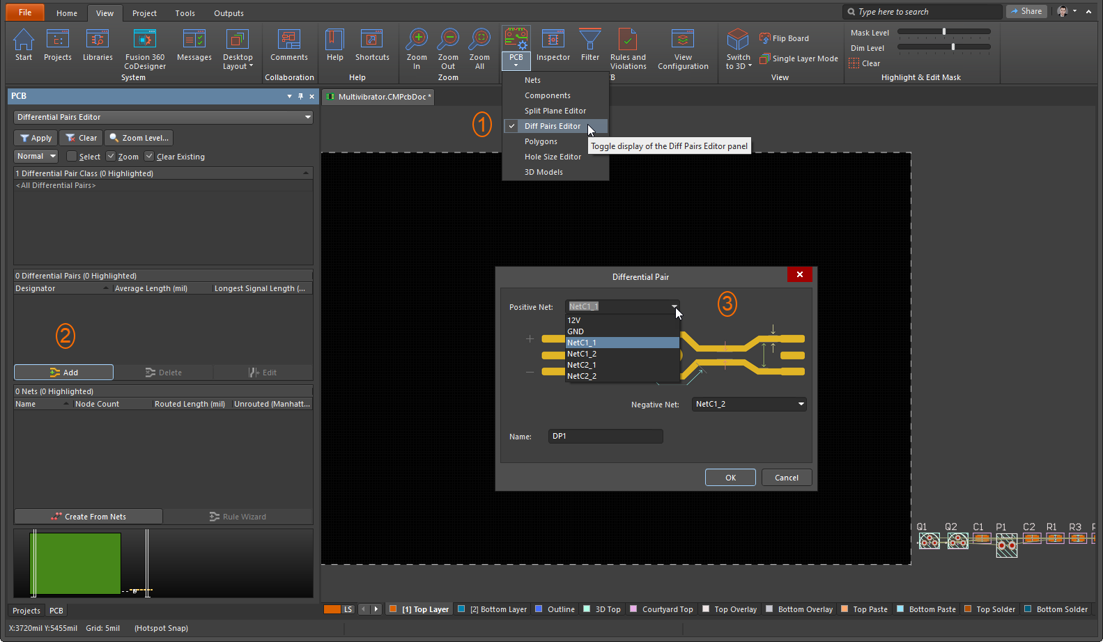
However, if nets were not defined as differential pairs on the schematic, you can also do this in the PCB editor. To do so, open the PCB panel then select Differential Pairs Editor or select it from the View | PCB | PCB drop-down menu (1). Use the Add button (2) to add a differential pair. From the Differential Pair dialog that opens, configure electric nets as positive or negative differential pair nets and assign them a name.
In the Design Rule Checker (DRC) dialog (Home | Design Rules | Run DRC » Design Rule Check), you can configure design rule checking for the board. All existing rules are listed and the Online (during design) and Batch (creates an optional report) columns indicate the type of check that will de performed. It is recommended to specify the minimum number of rules to be checked online to keep the system efficient. It is recommended to configure Clearance (in Electrical), Differential Pairs Routing and Width (in Routing) for Online checking.

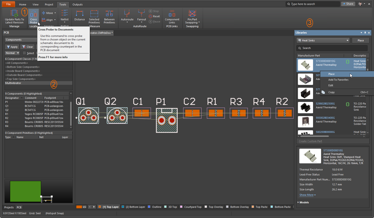
Components transferred from the schematic will be grouped and divided in the same way as in schematic documents, which is by sheets. You can use the Cross Probe (1) tool to navigate between schematic and PCB documents. Use the Shift+C shortcut keys to remove the selection if necessary.
For quick access to any component, you can use the Components mode of the PCB panel in which different component classes are presented in the upper area, including system classes (such as by the board layer on which components are placed) and user-defined classes (for example, generated by schematic sheets on which components are placed). In the lower region, components are grouped by the selected category (2).
If you need to place a component directly onto the board, you can drag it or use the Place command from the Libraries panel (3). Such components will not be connected to the schematic, therefore, this method of placement is used only when it is necessary to place a mechanical element, such as a heater.
Before you start routing, you should define the necessary parameters of conductors, clearances, and vias. These steps are executed from the various routing rules provided in the PCB Rules and Constraints Editor. These rules determine the minimum, maximum, and preferred dimensions of tracks, and holes, as well as the minimum clearance between topological elements.

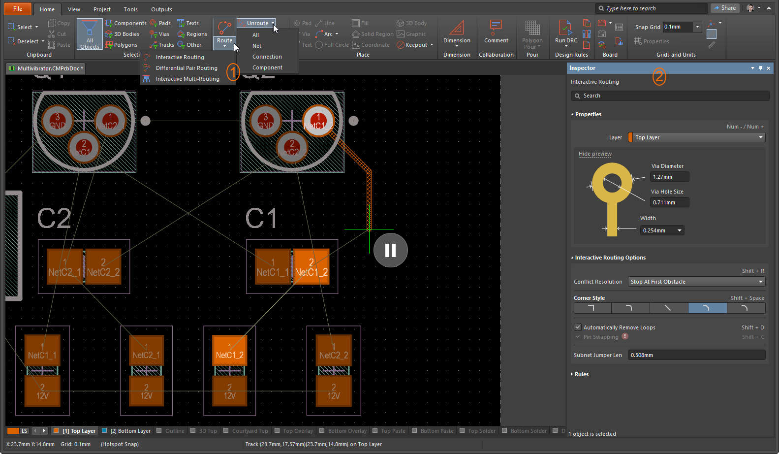
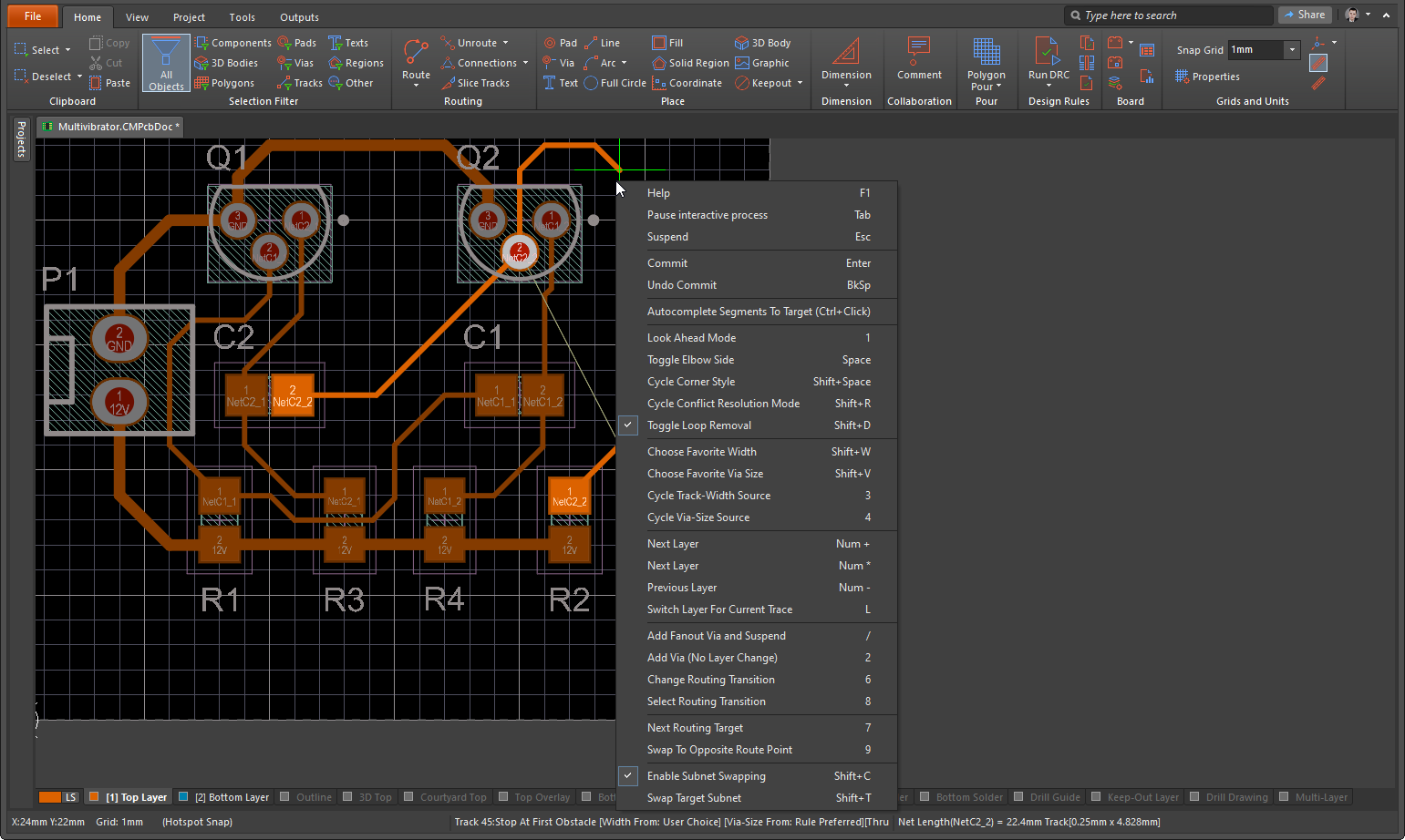
Routing and track removal commands are located in the Routing region of the Home tab. Their respective drop-down menus contain various options (1).
The Shift+Space keyboard shortcut changes the routing style while active routing. You can use the Tab key to pause and select parameters in the Inspector panel (2) if you need to change track parameters when routing. You can also change the corner style, thickness, via parameters, etc. The options for the routing style are 45 degrees, 45 degrees with an arc, 90 degrees, and 90 degrees with an arc or angle.
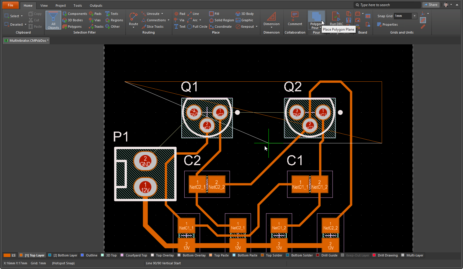
Polygons are created by using the Polygon Pour Cutout command in the Home | Pour | Polygon Pour drop-down. During placement, use the Shift+Space keyboard shortcut to cycle through the available corner modes.
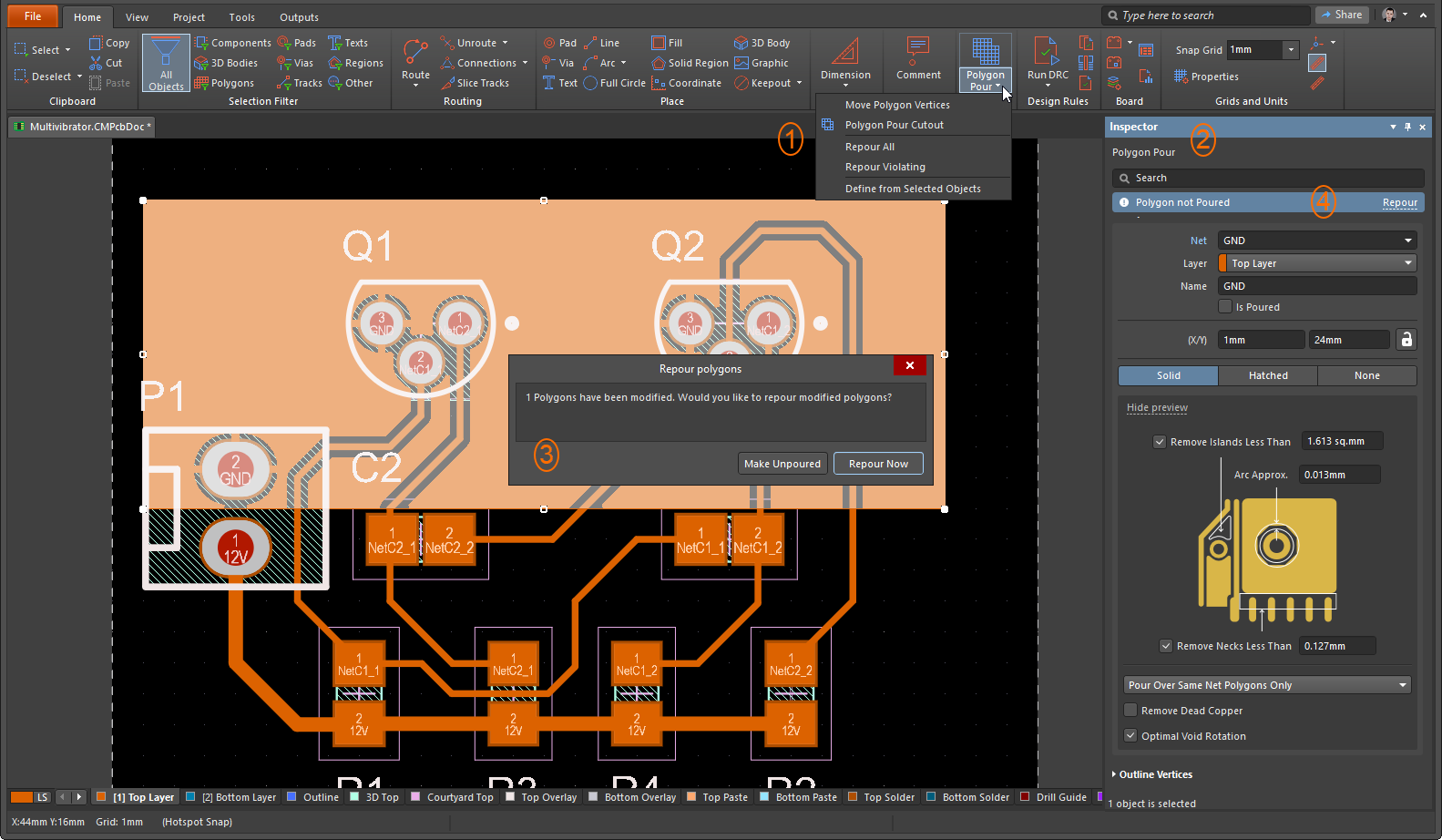
You can move a selected polygon and repour polygons using commands in the drop-down. The name, layer and net are configured in the Inspector (2) panel.
When edits are made to a polygon, a dialog opens in which you can choose to repour the modified polygon. You can also use the Repour (4) command in the Inspector panel.
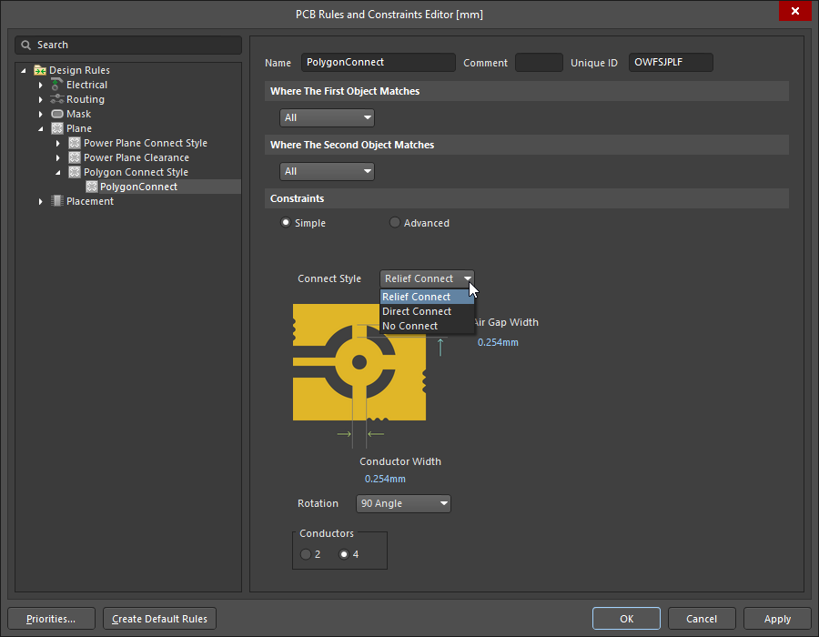
You can connect the polygon to the pads using the Connect Style drop-down in the PolygonConnect rule in the PCB Rules and Constraints Editor.
Even the most simple projects require PCB checks. Errors that can go unnoticed will be found with the well-established system of rule analysis and violation detection.
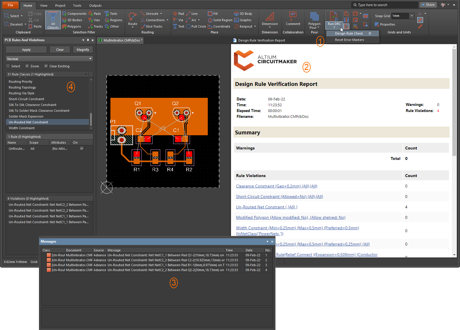
In the drop-down menu of the Run DRC button are commands to run the Design Rules Check and an option to Reset Error Markers (1).
After the check is complete, you can view the rule violations that were found in the Design Rules Verification Report (2), the Messages panel (3) and the PCB Rules And Violations panel (4).
In the PCB Rules And Violations panel, select a rule in the Rules region to display all violations of that rule in the Violations region of the panel. Double-click a violation to highlight the violation on the PCB. When you double-click on a violation in the panel, the Violation Details dialog opens so you can see the violation in detail.
The PCB editor has its own set of keyboard shortcuts. Some of the commonly used keyboard shortcuts in the PCB editor include:
The list of commands varies depending on the types of active documents.
Click View | Shortcuts to open the Shortcuts panel. Use the controls at the top of the panel to sort by name, category of actions to be executed, or alphabetical order.

Contact our corporate or local offices directly.
