Created: July 30, 2020 | Updated: February 11, 2022
What are PCB & PCBLIB Editor UI Elements?
PCB & PCBLIB Editor UI elements are ribbons and commands that are accessible when working in the PCB and PCB Library editors.
For ribbon commands that are specific to other editors (SCH, SCHLIB, Layer Stack, Component, etc.,), refer to those editors using the documentation navigation tree.
For ribbon commands that are general in nature (e.g., panel access, saving projects, printing, etc.,), refer to Common UI Elements.
Elements of the PCB and PCBLIB Environments
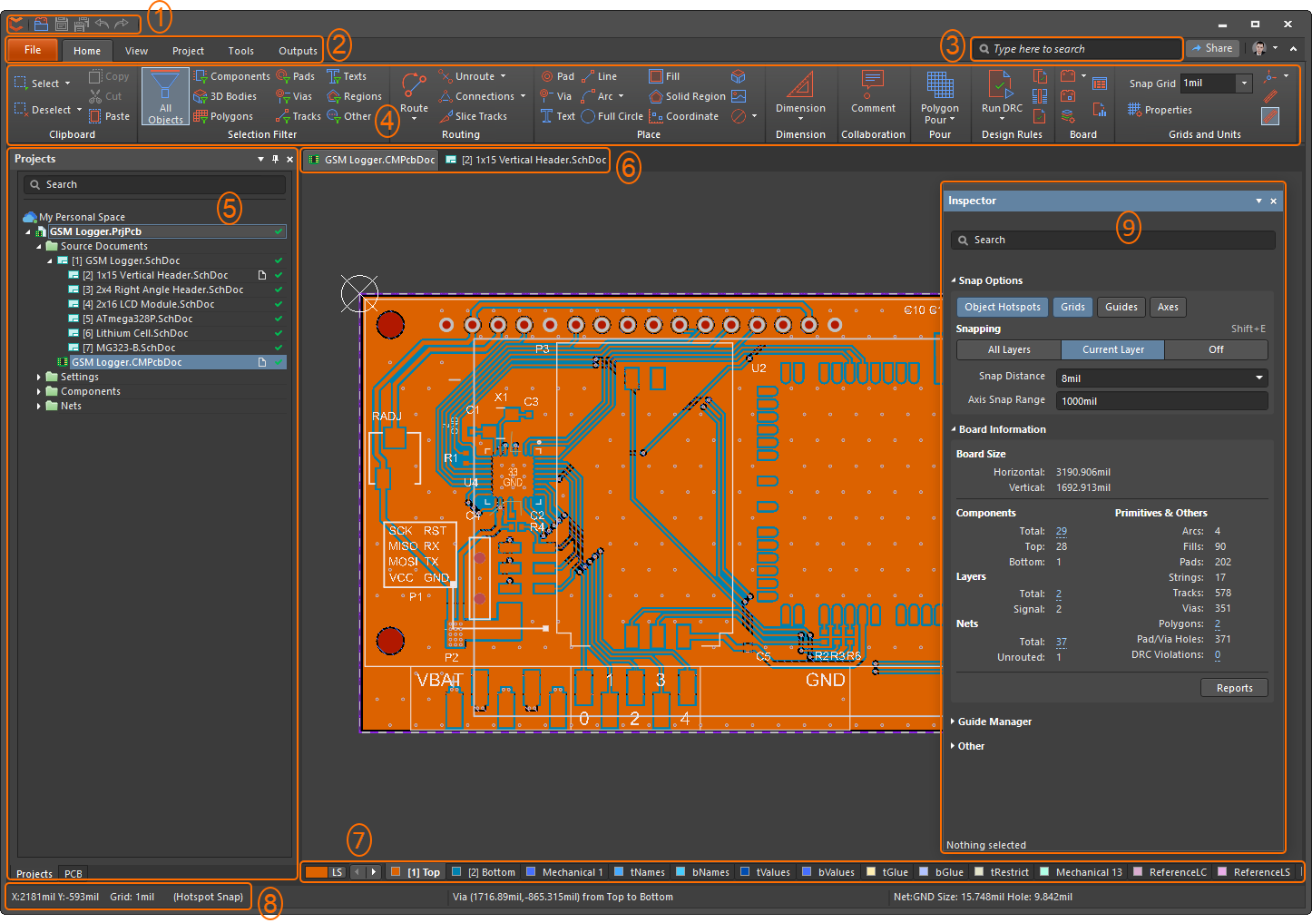
Quick Access Bar - click the icons to close and exit CircuitMaker, open existing projects, save the active document or all documents, and undo/redo the last commands
PCB editor tabs - each tab includes its own ribbon and commands.
Search - enter a search string in the field to access a command, panel, dialog, etc.
Ribbons and commands - use to perform various commands and functions in the PCB editor.
Pinned/docked panel.
Document tabs - displays the currently open documents. The active document displays with a gray background (GSM Logger.CMPcbDoc in the image). Click on a tab to open it in the design space and make it the active document.
Floating panel.
Layer tabs - displays all the layers of the PCB. The active layer displays with a gray background ([1] Top in the image). Click on a tab to show it in the design space and make it the active layer.
Status bar - displays the current X/Y location, the grid value, and the snapping mode.